Discover how artificial intelligence optimizes PCB assembly through smart inspection, defect detection, and predictive maintenance to boost yield and slash production costs.
Artificial Intelligence in PCB Assembly Optimization
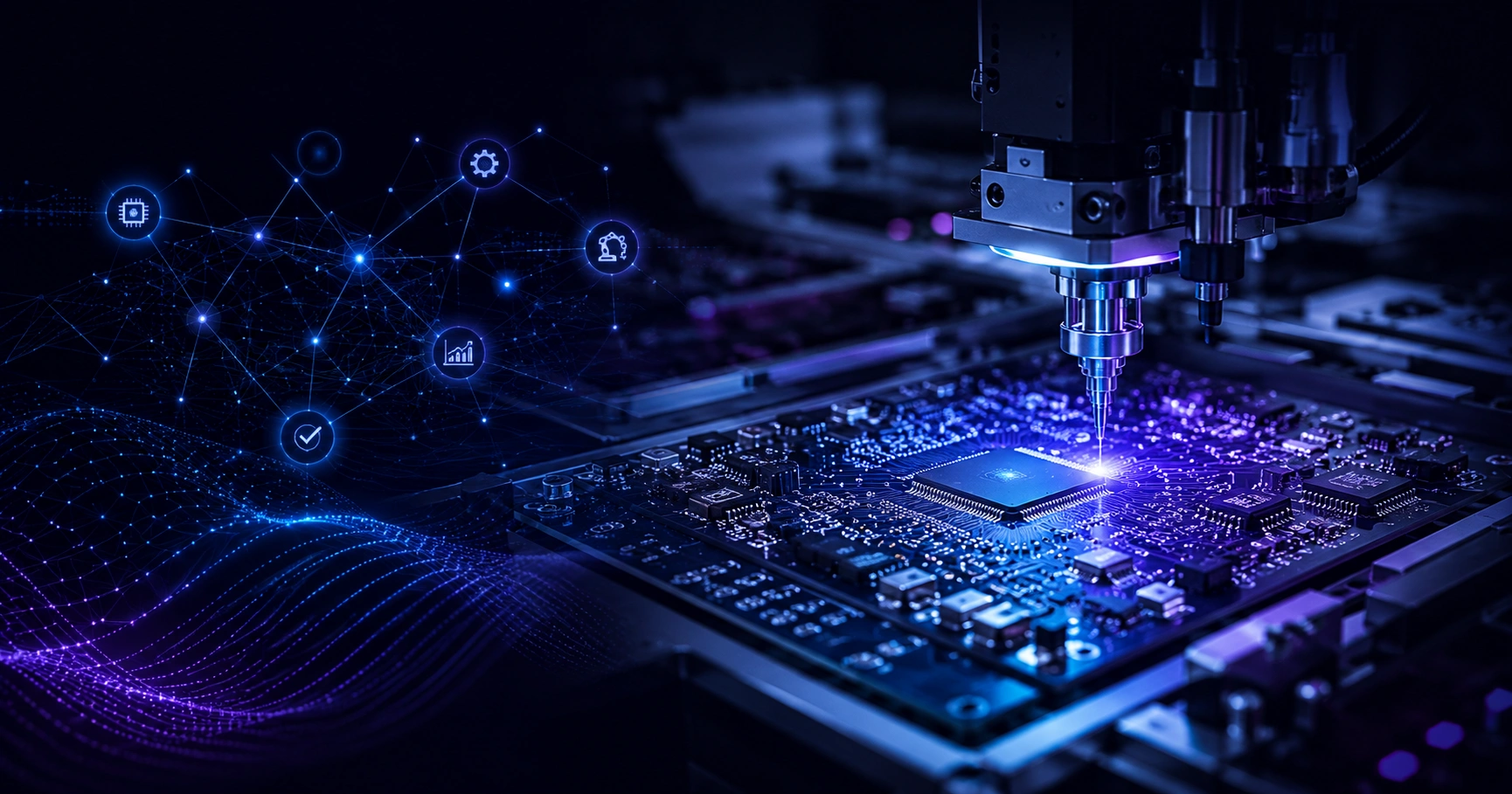
Printed circuit board (PCB) assembly is one of the most precision-dependent processes in modern electronics manufacturing. A single misplaced 0201 component or a hairline solder defect can render an entire board useless. As boards shrink and component density climbs, human inspection alone can no longer keep pace. This is exactly where artificial intelligence is reshaping the factory floor. Having worked alongside SMT (surface mount technology) production teams, I have seen AI move from a buzzword to a daily tool that catches defects engineers physically cannot see.
In this guide, we break down how AI optimizes PCB assembly end to end, the measurable gains it delivers, and how manufacturers can adopt it without disrupting existing lines.
Quick Answer: Artificial intelligence optimizes PCB assembly by using machine vision and machine learning to detect defects, optimize component placement, and predict equipment failures. The result is higher yield, fewer escapes, reduced rework, and faster throughput compared with manual or rules-based inspection methods.
What Does AI Actually Do in PCB Assembly?
AI in PCB assembly refers to the use of machine learning, computer vision, and predictive analytics to automate decisions that once relied on human judgment. Instead of fixed rules, AI models learn from thousands of labeled board images and sensor readings, improving accuracy over time.
The core jobs AI handles on a modern SMT line include:
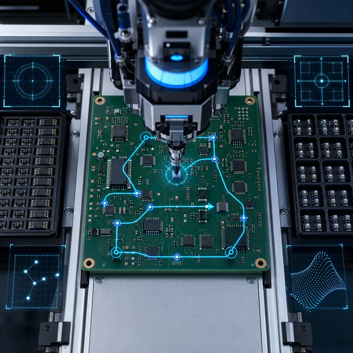
- Automated Optical Inspection (AOI): Identifying solder bridges, tombstoning, missing components, and misalignment.
- Component placement optimization: Calculating the fastest, most accurate nozzle paths.
- Predictive maintenance: Flagging machines before they fail.
- Process control: Adjusting reflow profiles and paste deposition in real time.
Unlike traditional rules-based systems that generate excessive false calls, AI learns the difference between a genuine defect and acceptable visual variation. This single capability is why adoption has accelerated so quickly across contract manufacturers.
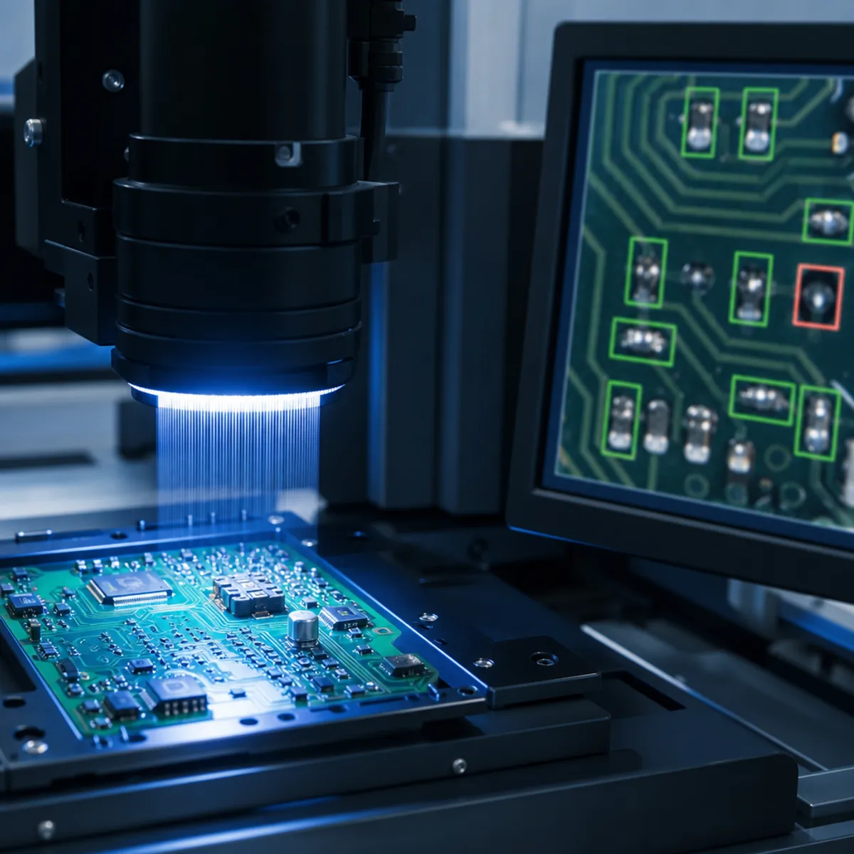
AI-Powered Inspection: The Biggest Win
Inspection is where AI delivers its most immediate return. Legacy AOI systems rely on rigid thresholds, so they flag harmless variations as defects, forcing operators to manually review hundreds of false alarms per shift. AI-driven vision systems dramatically reduce this noise.
According to IPC industry data, inspection and rework can account for up to 30 percent of total PCB manufacturing cost. By cutting false-call rates, AI lets skilled operators focus only on genuine issues. In practice, teams I have worked with reduced false calls by more than half within the first few weeks of deploying a trained vision model.
How Machine Vision Reads a Board
A deep learning model is trained on labeled images showing both good and defective joints. During production, high-resolution cameras capture each board, and the model classifies every solder joint in milliseconds. Because the model generalizes from patterns rather than fixed pixel thresholds, it tolerates lighting shifts and minor cosmetic differences that would trip a rules-based system.
Machine Learning for Defect Detection and Root Cause
Defect detection is the most mature AI application in PCB assembly, and modern models now identify defect types that escaped earlier systems.
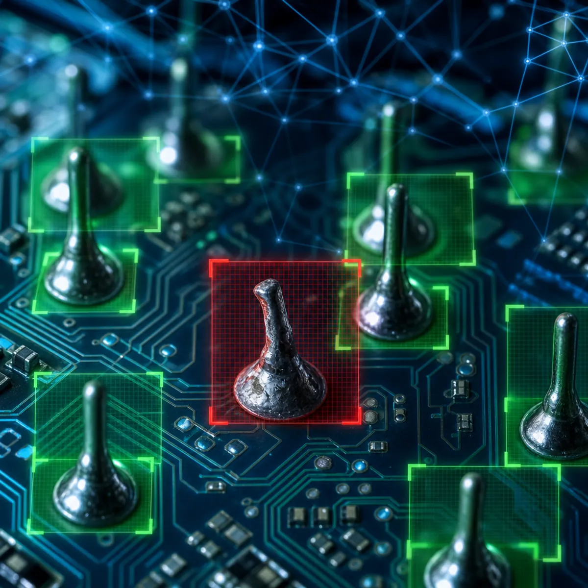
Beyond simply flagging a fault, AI connects defects back to their source. If tombstoning spikes on a specific feeder, the system correlates the pattern and alerts engineers before the trend becomes a scrap event. This shift from reactive to predictive quality control is the real competitive advantage.
Common defects AI reliably catches include:
- Solder bridging between adjacent pads
- Tombstoning, where a component lifts on one end
- Insufficient or excess solder
- Missing or misaligned components
- Lifted leads and cold joints
For manufacturers building AI-driven quality systems, partnering with specialists such as the team at ZoneTechify's artificial intelligence services can shorten the path from pilot to production-grade deployment.
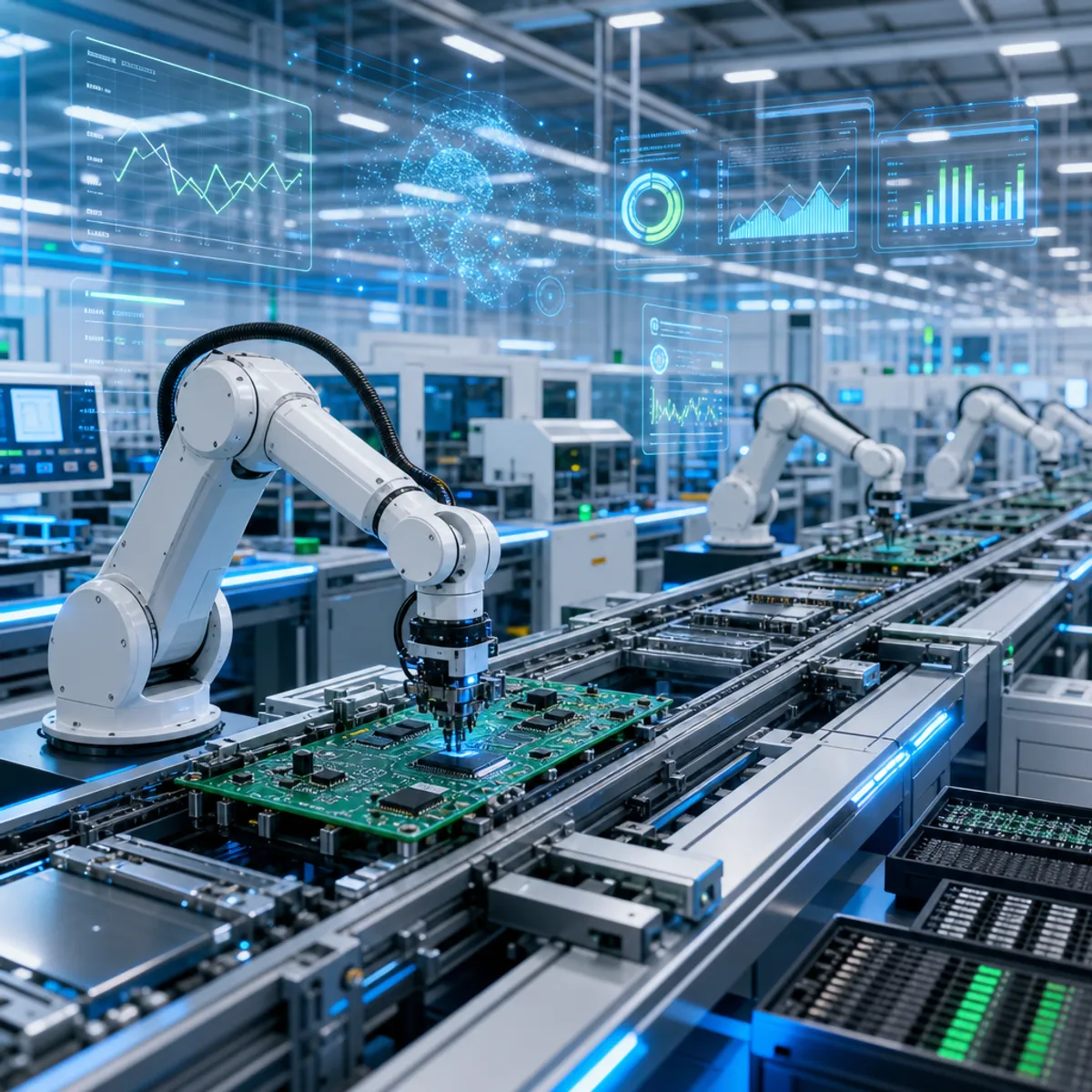
Optimizing Component Placement and Throughput
Component placement is a hidden bottleneck. A pick-and-place machine may handle tens of thousands of placements per hour, and the order and route of those placements directly affects cycle time.
AI optimization algorithms calculate the most efficient nozzle assignments, feeder layouts, and travel paths. By minimizing head movement and tool changes, these systems can meaningfully increase placements per hour without new hardware. The gain compounds across millions of units, turning a software upgrade into measurable capacity expansion.
This is a classic optimization problem, similar to the traveling salesman challenge, where AI evaluates countless combinations far faster than any human planner. The output is a placement program tuned for both speed and accuracy.
Predictive Maintenance: Stopping Downtime Before It Happens
Unplanned downtime is one of the costliest events in electronics manufacturing. A stalled SMT line can idle an entire production cell. AI-driven predictive maintenance changes the equation by monitoring vibration, temperature, motor current, and nozzle wear in real time.

Machine learning models detect subtle anomalies that precede failure, prompting maintenance during scheduled windows rather than mid-run. According to Deloitte research, predictive maintenance can reduce equipment downtime by up to 50 percent and extend machine life by years. For a high-mix, high-volume facility, that reliability translates directly into on-time delivery and protected margins.
Real-Time Process Control and Quality Assurance
AI does not just inspect finished boards; it actively steers the process. By analyzing data from solder paste inspection, placement, and reflow simultaneously, AI closes the loop between stages.

For example, if solder paste inspection detects a deposition drift, the system can recommend or trigger a stencil cleaning before defective boards are ever assembled. This real-time feedback prevents defects rather than catching them afterward, which is the difference between scrapping a board and never producing a bad one.
AI vs Traditional PCB Assembly Methods
The contrast between AI-enhanced and conventional approaches is stark. The table below summarizes the practical differences manufacturers experience.
| Factor | Traditional Rules-Based Method | AI-Optimized Method |
|---|---|---|
| Defect detection accuracy | Moderate, misses subtle faults | High, learns over time |
| False-call rate | High, heavy manual review | Low, focused review |
| Adapts to new boards | Manual reprogramming | Learns from new data |
| Placement optimization | Static, operator-set | Dynamic, route-optimized |
| Maintenance approach | Reactive or scheduled | Predictive |
| Cost over time | Rises with complexity | Falls as models mature |
The key takeaway is that AI systems improve as they ingest more data, while traditional systems remain static unless manually reconfigured.
How to Start Implementing AI in PCB Assembly
Adopting AI does not require replacing an entire line overnight. Based on real deployments, a phased approach works best:
- Audit your data: Collect and label historical inspection images and machine logs.
- Start with inspection: Deploy AI on AOI first, since it offers the fastest, most visible ROI.
- Integrate gradually: Add placement optimization and predictive maintenance once inspection is stable.
- Train your team: Operators must learn to validate and retrain models, not just monitor them.
- Measure relentlessly: Track yield, false-call rate, and downtime before and after deployment.
The businesses that succeed treat AI as a continuous improvement program, not a one-time install. Resources like WebPeak and the specialists behind WebPeak's artificial intelligence services can help teams design data pipelines and integration strategies that scale with production volume.
The Future of AI in Electronics Manufacturing
The trajectory is clear: AI is moving from isolated inspection stations to fully connected, self-optimizing lines. Generative models are beginning to suggest design-for-manufacturability improvements before a board even reaches production.
As digital twins, edge AI, and Industry 4.0 platforms converge, factories will simulate and optimize entire assembly runs virtually before committing materials. Manufacturers who build AI competency now will hold a durable advantage as boards grow denser and tolerances tighten further.
Key Takeaways
- AI optimizes PCB assembly across inspection, placement, maintenance, and process control.
- Inspection delivers the fastest ROI, cutting false calls and focusing skilled labor on real defects.
- Inspection and rework can represent up to 30 percent of PCB manufacturing cost, per IPC data.
- Predictive maintenance can cut downtime by up to 50 percent, according to Deloitte.
- AI systems improve continuously as they learn from new production data.
- A phased rollout, starting with AOI, minimizes risk and maximizes early wins.
Frequently Asked Questions (FAQ)
How does AI improve PCB assembly quality?
AI improves PCB assembly quality by using machine vision and machine learning to detect defects more accurately than rules-based systems. It reduces false calls, catches subtle solder issues, and links defects to root causes, allowing manufacturers to fix problems before they create scrap or field failures.
Is AI in PCB assembly expensive to implement?
Upfront costs exist, but AI typically pays back quickly through reduced rework, higher yield, and less downtime. Most manufacturers start with AI-powered inspection because it offers the fastest return, then expand into placement optimization and predictive maintenance as confidence and data maturity grow.
Can AI replace human inspectors completely?
No, AI augments rather than fully replaces human inspectors. It handles repetitive, high-speed classification while skilled engineers validate edge cases, retrain models, and make final judgment calls. The most effective setups pair AI's consistency with human expertise for continuous improvement and accountability.
What defects can AI detect in PCB assembly?
AI reliably detects solder bridging, tombstoning, insufficient or excess solder, missing or misaligned components, lifted leads, and cold joints. Because models learn from labeled examples, they also identify subtle or rare defects that fixed-threshold optical systems frequently miss during high-volume production runs.
How do I start using AI on my SMT line?
Begin by collecting and labeling historical inspection images and machine data. Deploy AI on automated optical inspection first for fast ROI, then expand into placement optimization and predictive maintenance. Train operators to validate and retrain models, and measure yield and downtime to prove results.